
  |
Enhanced GaN mis-hemt has not been commercialized successfully. The interface state between GaN and dielectric is one of the main factors that restrict the reliability of devices.
Previous studies have found that LPCVD SiNx has the advantages of high temperature resistance, high film quality, compact structure, no ion damage and high TDDB characteristics, which is expected to be used as gate dielectric and passivation material for highly reliable mis-hemt. However, the high growth temperature of traditional LPCVD SiNx may lead to thermal decomposition and reaction on the material surface, especially the etched surface. At the same time, high temperature process (for example, ohmic alloy above 800 ℃) will lead to the destruction of hydrogen bond at passivation site, which leads to the degradation of dielectric interface to a certain extent, resulting in disordered rough crystallization region with random change of bond length and bond angle and amorphous region with gradient change, resulting in uncontrollable frequency dispersion and hysteresis phenomenon.
In order to avoid these disadvantages, the strong interface needs to have atomic level flatness and a long-range ordered crystal region with minimum degeneration.
On the other hand, due to the wide distribution of defect electron capture cross sections in wide band gap semiconductors, the frequency dispersion and current collapse may be affected by the interface states of ultra shallow and deep levels.
Therefore, it is very meaningful to evaluate the interface states in a wider energy range. Constant capacitance deep level transient Fourier spectroscopy can be used to measure the temperature range of 10 ~ 400k, which provides an effective characterization solution for the above requirements.
However, the detection density of interface state and discrete energy level defects in multilayer materials is usually coupled, which makes the defect analysis of dielectric / III-N interface more complicated. It is necessary to separate interface state and discrete defect energy level by using interface state distribution function. Although the U-type model based on digs theory is suitable for the interface state distribution of continuous energy levels, there are still some limitations in the wider energy range.
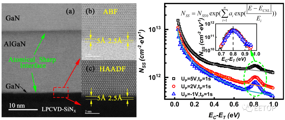 Density of States and U-shape distribution function of atomic level flat interface and advanced level interface This work proves that low heat budget process is one of the effective means to achieve high quality interface, including: LPCVD SiNx growth temperature is reduced from 780 ℃ to 650 ℃, ohmic alloy temperature is reduced from 850 ℃ to 780 ℃. The difficulty is to reduce the temperature window and ensure high quality film and ohmic contact.
Finally, a 2.5-5 nm atomic level flat interface is achieved between LPCVD SiNx and GaN. The interface density of States is about 1.5 × 1013 cm-2ev-1 at et = 30 MeV and about 4 × 10¹¹ ~ 1.2 × 1012 cm-2ev-1 at et = 1 eV.
The team innovatively proposed a U-shaped distribution function of interface states based on physical parameters, which is suitable for a wide energy range, and realized the effective separation of discrete energy levels and interface states in multilayer materials. The achievement was published in applied surface science with the title of "suppression and characterization of interface states at low-pressure-chemical-vapor-deposited SiNx / III-nitride heterostructures". ( DOI:10.1016/j.apsusc.2020.148530 )。
This work is supported by the National Natural Science Foundation of China's major instrument projects, key projects, general projects and the Chinese Academy of Sciences frontier key projects.
Related paper links: https://www.sciencedirect.com/science/article/abs/pii/S0169433220332888 |
All contents are reproduced in all forms without written permission.© Copyright 2017 Wuxi Zhuohai Technology. All rights reserved. | 苏ICP备10225498号-2
We recommend that you use IE8.0 and above browser to visit this site.![]()